
Improving EMC performance in switched-mode power supplies
Switched-mode power supplies (SMPS) are in high demand due to their high efficiency and power density. However, they can often cause problems with conducted and radiated emissions during EMC verification. To avoid these problems, SMPS can be equipped with snubber circuits to help them pass EMC certification.
Keeping oscillations on PCBs under control
The performance of a product can be impaired if undesirable voltage or current peaks (ringing) occur on the PCBs. These oscillations are caused by the leakage induction of the transformer in conjunction with parasitic capacitances of the switching element itself and the PCB.
Snubbers are used in electronic circuits across switching or rectifier elements to suppress unwanted ringing and increase the reliability and service life of the circuit. The snubbers can be located on both the primary and secondary side of a SMPS.
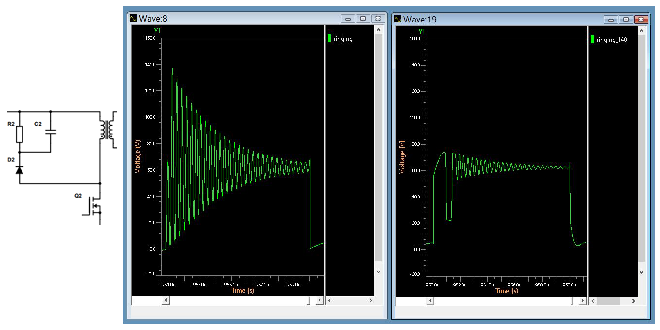
This example shows an isolated DC/DC converter using the UCC3809 controller and circuitry according to the reference design. On the primary side of the transformer, a resistor-capacitor-diode snubber (RCD snubber) is placed, while on the secondary side a resistor-capacitor snubber (RC snubber) is populated.
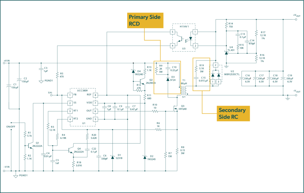
The most common snubber types
The simulation diagrams show the voltage-time behavior before and after the different snubbers are inserted:
- RC snubber: An easy-to-use snubber that reduces both the amplitude as well as the duration of the ringing.
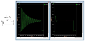

- Rate of rise snubber: The rate of the voltage change across a switching element is reduced, wich also reduces the amplitude of the voltage across the element.
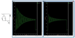

- Clamp snubber: The voltage peaks across the switching element (Q2) are clamped back to the input voltage, which results in lowering the stress on the component itself.


Drawbacks when using snubbers
The exact design and positioning of a snubber depends on the specific requirements and conditions of the circuit in question. It is therefore important to weigh up exactly when and in which version a snubber makes sense. In addition to a number of additional components, a snubber also requires space on the circuit board. Probably the biggest challenge, however, is the power loss caused by a snubber, which reduces the efficiency of the power supply and generates unwanted heat in the system. It is therefore always a tradeoff between power loss and EMC performance.
Due to the parasitic side effects of the switching elements and the PCB, selecting the right components is usually not a simple process. Thus, it is necessary to fine-tune the final PCB components using tools such as a fast oscilloscope.
Important considerations for successful use
To ensure that a snubber functions properly, the following points must be taken into consideration:
- The snubber components must be placed close to the switching element. This minimizes loops (inductivities) and reduces parasitic effects of the conductor tracks and the PCB itself.
- Calculate the expected snubber components beforehand.
- Verify the proper behavior of the snubber components in the final design, as calculations and simulations may differ from reality. Adjust the components if necessary.
- Check the losses in the snubber resistors as they tend to heat up, especially if they are effective in reducing the ringing.
- Select the correct voltage rating of the capacitor, as high voltage peaks may occur.
Do you need support for your electronic circuits? Then please do not hesitate to contact us. We are happy to provide support from the design stage through to development and are available to our customers as a partner throughout the entire product life cycle.
______________________________________________________________________________
Author:
Daniel Gugelmann, Senior Embedded Systems Engineer
We are here for you – send us your request!
Developing together! We put your ideas into practice and accompany your projects until they are ready for the market. Get in touch with our experts now.

